Across nearly every advanced engineering sector, the pressure to deliver smaller, lighter, and smarter devices is accelerating.
Medical implants are becoming less invasive yet more capable. Aerospace and defense systems require compact components that reduce weight without sacrificing strength or performance. Consumer electronics continue to pack more processing power into thinner and more portable form factors. Even industrial and automotive systems are undergoing a redesign toward compact, integrated components that support higher efficiency and reliability.
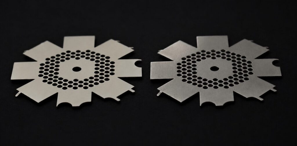
At the center of this miniaturization trend is the rise of micro-features – ultra-fine geometries measured in microns, patterns with extremely high density, and thin-metal structures that enable unprecedented levels of functionality. These features are no longer optional. They are foundational to performance, reliability, and multi-function integration.
In this article, we explore what micro-features are, why they matter, and how Microphoto’s fully Tabless workflow is redefining what’s possible for next-generation aerospace, medical, defense, and electronics applications.
In engineering terms, micro-features refer to extremely small geometries that enable compact, high-performance systems. These include:
These features allow engineers to create parts with intricate designs, improved surface performance, and integrated functionality that traditional fabrication methods simply cannot match.
Legacy fabrication methods, such as machining, metal stamping, sheet metal stamping, and laser cutting, begin to break down when engineers push into micro-scale geometries. As tools wear, dimensional accuracy shifts, causing inconsistencies across metal sheets. Mechanical stress from punches or cutting forces can distort thin materials, while burr formation compromises delicate surfaces and edge quality.
Stamping presses are also limited by minimum punch sizes, preventing the creation of ultra-fine apertures or high-density arrays. Laser cutting introduces tapered edges and heat-affected zones, altering the material surface and restricting achievable intricacy. Meanwhile, miniature EDM processes suffer from slow cycle times, making them impractical for dense or complex feature sets.
As micro-features shrink and metal thicknesses decrease, these challenges quickly become engineering barriers that limit what traditional manufacturing can reliably create. The photochemical etching process removes these constraints by eliminating mechanical force, thermal distortion, and tool-based limitations.
This enables engineers to create parts with ultra-fine geometries, intricate designs, and repeatable high-density patterns, delivering the advantages needed for modern aerospace, medical, automotive, electronics, and other precision-driven industries as they scale into next-generation production.
Micro-features are enabling breakthroughs in nearly every advanced sector. Whether the application is aerospace, electronics, medical, or industrial, the demand for smaller, lighter, more integrated components is reshaping product design. Here’s how:
As medical technology becomes smaller and more intelligent, micro-fabricated components are becoming essential.
These features enable minimally invasive devices, improved patient outcomes, and more compact implantable technologies.
The aerospace and defense industries depend on micro-features to reduce weight, integrate multi-functionality, and improve system performance.
In these applications, reliability, precision, and predictable performance at production scale are essential.
Miniaturization continues to transform the electronics world.
Many of these micro-features cannot be produced via machining or stamping without defects or distortion.
Emerging products rely heavily on micro-fabricated metal features:
These innovations require light, compact, thermally stable components produced from advanced materials without compromising performance.
Photochemical etching (PCM) stands out as one of the only processes capable of producing micro-features reliably, affordably, and at high-volume manufacturing scale.
The etching process uniquely enables complex, delicate geometries at scale where other techniques fail.
|
Method |
Limitations |
|
Miniature stamping |
Tool wear, burrs, mechanical distortion, poor performance at extremely small sizes |
|
Laser cutting |
Heat-affected zones, taper, inconsistent edges at micro scale |
|
EDM |
Slow, expensive, unsuitable for multi-feature arrays |
|
CNC machining |
Tool breakage, minimum size constraints |
Microphoto is the only U.S. photochemical etching provider engineered around a fully tabless workflow. For micro-features, this is a major differentiator, and here’s why:
Traditional etching uses hold-tabs to anchor parts to the metal sheet. At the micro level, tabs introduce:
Microphoto’s tabless workflow eliminates these issues entirely, offering:
This results in superior micro-features that maintain integrity from R&D through scaled production.
Engineers designing micro-scale metal components must rethink traditional design assumptions. As features shrink and density increases, factors like etch geometry, material behavior, tolerances, and pattern uniformity become far more influential on final part performance. The etching process offers greater freedom than mechanical methods, but achieving optimal results requires understanding how chemistry interacts with metal sheets, material thickness, and feature layout.
Below are the core considerations engineers should evaluate when designing micro-etched features for next-generation miniature devices.
A general rule: finer features require thinner metals. Understanding the etch factor and its effect on lateral undercut is essential for predictable outcomes.
High aspect ratios allow high-density micro-patterns but must align with material tolerance limits.
The ratio of vertical to lateral etching determines wall geometry and opening profile. Designs must be balanced to achieve straight, uniform edges.
Each material brings different mechanical and chemical characteristics.
Rounded interior corners often perform better than sharp ones at micro scale due to etch behavior and stress distribution.
Uniformity is essential for micro-screens, micro-filters, and sensor grids. Photochemical etching naturally excels at sheet-level uniformity.
Photochemical etching is the most efficient path from prototype to production for miniaturized components because it requires no tooling, enabling immediate design iteration while using the exact same etching process at every stage of development.
This consistency ensures predictable scaling, highly repeatable tolerances even across dense arrays, and rapid engineering cycles to refine micro-features without costly delays.
With reduced costs at small and medium volumes and seamless transition into full-scale manufacturing, Microphoto combines fast-turn prototyping with reliable production capacity, making it an ideal long-term partner for next-generation device development.
As industries push the limits of performance, miniaturization will continue to accelerate. Some of the key trends that are predicted include:
Photochemical etching will remain essential as devices grow smaller, lighter, and more complex.
The next generation of aerospace, medical, defense, automotive, and electronics devices will be defined by micro-features. Few fabrication methods can support these materials, geometries, and tolerances at scale. The photochemical etching process is one of them.
Microphoto’s tabless, precision-first workflow offers engineers the accuracy, consistency, and manufacturing reliability required to build future-ready components. Whether you are developing ultra-fine screens, micro-interconnects, precision filters, miniature springs, or integrated photonic structures, Microphoto’s trusted team delivers the advantages needed to take your project from concept through production with confidence.
Contact the Microphoto team today to discuss your project or request a quote.