As electronic devices get smaller and more powerful, the battle against electromagnetic and radio-frequency interference has intensified. Today’s compact, high-speed devices pack more electronic components into tighter spaces than ever before, increasing the risk of signal degradation, performance instability, and outright failure.
That’s why EMI shielding plays such a critical role in the design of modern electronics. Whether it’s consumer electronics, medical devices, defence systems, or industrial instrumentation, the ability to block or redirect unwanted electromagnetic waves is vital to maintaining reliability and meeting regulatory standards.
At Microphoto, we specialise in photochemical etching of thin-metal EMI/RFI shielding solutions engineered for the unique challenges of miniaturized devices. With decades of experience supporting electronics, aerospace, defence, and medical manufacturers, we help our partners meet evolving performance and compliance demands with precision shielding components designed for tight enclosures.
In this article, we explain the impact of EMI, RFI, and electromagnetic energy on modern electronics, why miniaturization makes interference harder to control, and how board-level, photo‑etched shielding solutions improve performance.
Electromagnetic interference (EMI) and radio-frequency interference (RFI) refer to disruptions caused by unwanted electromagnetic radiation or signals. These disturbances can originate from internal sources (e.g., switching power supplies, high-speed data lines) or external environments (e.g., other nearby devices).
Uncontrolled EMI can lead to signal crosstalk, data loss, measurement errors, overheating, and even permanent damage to electronic components. In mission-critical applications—from aerospace navigation to medical monitoring—the cost of interference-related failure is steep.
RFI, which is a subset of EMI focused on higher-frequency radio waves, can be particularly problematic for wireless devices, GPS systems, and any application requiring clean signal transmission. Even trace levels of interference can reduce shielding effectiveness and impair system performance.
This type of interference can lead to:
Designers must account for electromagnetic interference (EMI) as a system-level risk and plan shielding strategies accordingly.
As demand for smarter, smaller, and more connected devices grows, so do the engineering challenges. Miniaturization significantly increases the difficulty of controlling EMI and RFI, so these types of electronics require shielding solutions that are both compact and precise, without sacrificing performance.
Some of the key issues caused by miniaturization include:
For most compact electronics, the most effective place to control EMI is at the board level.
Common board-level shielding elements include:
Precise fit and geometry are critical. Gaps, misalignments, or deformed shielding can compromise shielding effectiveness and cause hotspots or resonance issues.
Effective shielding starts at the design phase, where tight collaboration between electrical and mechanical teams is essential.
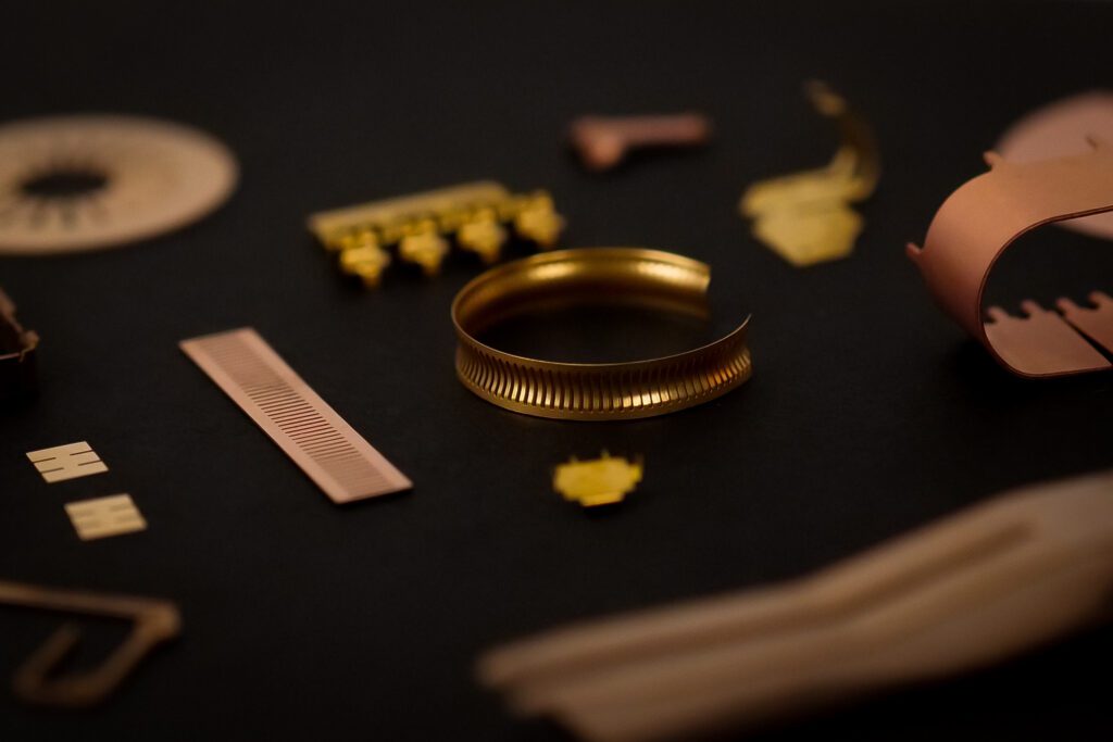
Photo-etched shielding components are uniquely suited for miniaturized electronics. The photochemical etching process enables highly detailed, low-profile metal parts with no mechanical stress, ideal for delicate or tightly packed designs.
Unlike stamped or machined components, photo-etched parts are free from burrs, warping, or deformation. This is especially important when installing over sensitive PCB traces or components.
Photochemical etching delivers exceptional dimensional accuracy. This ensures repeatable, flush fitment to enclosure walls or board standoffs—improving both EMI shielding effectiveness and mechanical integration.
Etched meshes can be produced with feature sizes down to a few thousandths of an inch, supporting airflow without compromising signal attenuation. These patterns also reduce weight and thermal buildup.
Etched shields are ideal for ultra-thin consumer electronics, wearables, or implantable medical devices where every millimeter counts.
The choice of emi shielding material directly impacts shielding effectiveness, manufacturability, and long-term durability.
Common EMI/RFI shielding materials include nickel silver, which offers high shielding performance and excellent corrosion resistance. Copper and copper alloys are also highly valued for their superior electrical conductivity and ease of forming. Another common material is stainless steel, which offers high strength and corrosion resistance, though it has lower electrical conductivity than copper-based materials.
When selecting EMI materials, engineers must consider:
Photochemical etching allows engineers to select from a broad range of metals and thicknesses without the constraints of stamping dies or machining setups.
Photo etching, or photochemical machining (PCM), uses UV light and etchants to selectively remove metal with extreme precision.
Advantages over traditional methods include:
Compared to machining or laser cutting, photochemical etching offers cleaner edges, better geometry control, and lower unit costs for thin-metal EMI shielding components.
Boasting over 60 years of experience, Microphoto has become a trusted partner to electronics OEMs and PCB designers seeking compact, high-performance EMI/RFI shielding solutions.
What sets us apart:
Our photo-etched EMI shielding gaskets, cans, and meshes are already used in thousands of applications worldwide, from handheld radios and smart sensors to avionics and implantable devices.
As electronic devices continue to shrink while operating at higher speeds and frequencies, controlling EMI and RFI must be treated as a core design requirement—not an afterthought. Interference issues introduced late in the development cycle can compromise performance, delay certifications, and increase redesign costs, particularly in compact, high‑density electronics.
Photo‑etched EMI/RFI shielding provides a proven path forward. By enabling ultra‑thin, precisely defined shielding cans, frames, and meshes, photochemical etching delivers consistent, repeatable interference protection at the board level—where space constraints and signal integrity demands are most acute. These low‑profile solutions integrate cleanly into modern enclosures while maintaining airflow, thermal performance, and mechanical reliability.
With unmatched dimensional precision, broad material flexibility, and a stress‑free manufacturing process, photochemical etching supports the next generation of miniaturized electronics—helping engineers achieve reliable EMI control without sacrificing design intent or manufacturability.
If you need precision RFI/EMI shielding solutions tailored to your application, Microphoto is the team to partner with. From early‑stage prototypes to full‑scale production, our team works closely with electronics manufacturers to deliver shielding components that perform under pressure – in any environment, at any scale.