Photochemical machining (PCM) is one of the most precise, flexible, and engineer-friendly fabrication technologies available for thin-metal components. While often compared to traditional machining methods such as laser cutting, stamping, or EDM, PCM stands apart for its ability to produce intricate, burr- and stress-free geometries without distortion, making it ideal for a range of critical applications.
But not all PCM providers operate the same way. As the only U.S. manufacturer purpose-built around a fully tabless workflow, Microphoto eliminates carrier tabs entirely, resulting in cleaner edges, higher yield, and more consistent repeatable parts.
In this article, we examine every stage of the photochemical machining process from design to finished part and explore the precision, repeatability, and cost-effectiveness that make it such a trusted process across industries.
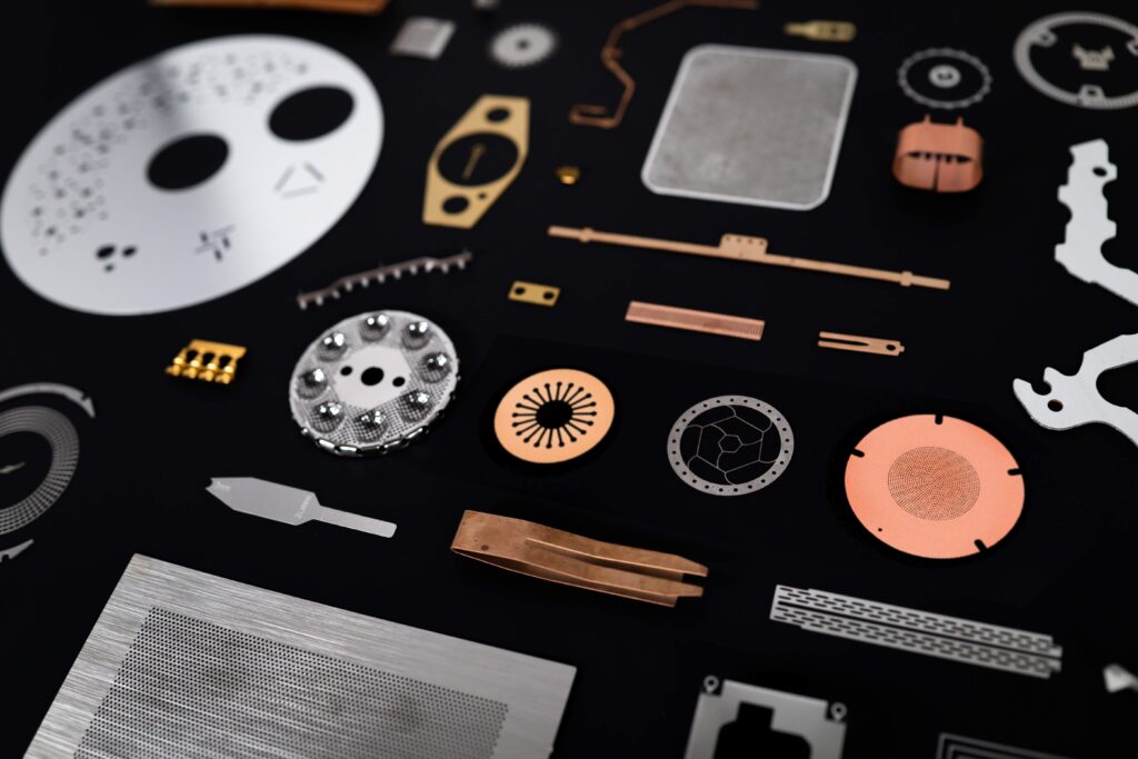
Photochemical machining is a subtractive manufacturing process that creates precision metal parts by selectively removing material from a metal sheet through a controlled chemical reaction. The approach uses a photoresist mask, UV-patterned artwork, and chemical etchants to generate the desired pattern without force, heat, or mechanical stress.
From an engineering perspective, PCM excels because:
Because PCM does not require hard tooling, design changes are inexpensive and fast, making the process ideal for programs with evolving requirements and aggressive development timelines. With its exclusive tabless process, Microphoto enhances these intrinsic benefits consistently producing cleaner edges, improving flatness, and eliminating post-processing steps that competitors must apply.
PCM is a precision-first manufacturing process that provides engineers, managers, and teams a low-risk, high-accuracy path for both prototyping and production.
The innovative etching process outperforms traditional fabrication when:
PCM becomes especially cost-effective compared to stamping, which requires hard tooling investments, even for simple prototype runs, or laser cutting, which struggles with microfeatures and can introduce taper or recast layers.
Every PCM project begins with digital design input, which can come in a range of file formats, including DXF, DWG, Gerber, PDF, and STEP. The engineering review stage is where manufacturability, material considerations, and application-specific requirements are aligned.
Early collaboration is essential because sharing application requirements, such as EMI shielding needs, spring action, flexure performance, battery tab behavior, thermal transfer, or biocompatibility, allows Microphoto to optimize design geometry before production begins.
Microphoto’s engineering team provides guidance during the specification stage, applying design-for-etching principles that reduce downstream variation and cost. As a result, customers and clients receive geometries refined for consistency, repeatability, and manufacturability long before the project moves deeper into the machining process.
Phototools are 1:1 scale films or digital masks generated directly from the customer’s CAD model. They define every feature of the part, including compensation for the etching factor and artwork shrinkage associated with coated-metal processing.
The expert team at Microphoto uses high-resolution photoplotters to create artwork with extremely fine detail, producing predictable results even with high-density designs.
During this stage, the metal sheet undergoes thorough cleaning to remove oils, oxides, and particulates that could interfere with photoresist adhesion, a critical requirement for maintaining uniformity throughout the etching process.
Surface preparation typically involves solvent degreasing, mechanical or chemical cleaning, and a controlled rinse-and-dry cycle to ensure the metal enters lamination in an ideal state. Once cleaned, the sheet is coated with a uniform layer of photosensitive resist. This even lamination is essential for achieving uniform etch rates, predictable wall profiles, and consistent feature definition across the entire panel.
This upstream discipline is fundamental to achieving repeatability. Microphoto’s controlled preparation workflow directly enhances tolerance stability, ensuring that every subsequent step of the photochemical machining process produces parts with the consistency and precision engineers depend on.
The phototool is aligned with the coated metal sheet and then exposed to UV light. UV hardens the photoresist in the areas defined by the artwork, while unexposed regions remain soluble.
Some of the critical aspects you need to be mindful of during this step include:
Precision at this stage directly correlates with the dimensional outcome of the finished part. Any misalignment or exposure variance translates into measurable part deviation.
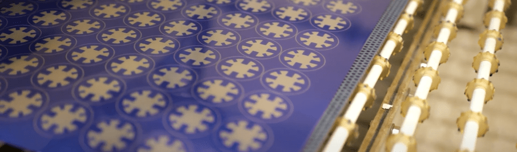
This stage is the core of the photo etching process, where chemical milling removes only the exposed metal areas to generate the intended geometry. The part enters a tightly controlled etching chamber, where parameters such as etchant temperature, chemistry, spray pressure, and dwell time dictate how quickly and uniformly material is removed. Only the unprotected metal dissolves, allowing the part to form exactly as defined by the phototool.
Several engineering factors play a major role in this step, including the etch factor (the relationship between lateral and vertical material removal), the material thickness and alloy, the required tolerances, and the undercut characteristics associated with high-aspect-ratio features. Each of these variables influences the final dimensional accuracy of the etched part, making this stage central to achieving consistent, high-precision metal etching.
Unlike traditional manufacturers that attach parts to a carrier frame with tabs, Microphoto performs etching entirely without carrier tabs. This eliminates everything from tab break-off marks and distortion near attachment points, to microcracks, post-processing deburring, and variability introduced by mechanical separation.
A tabless approach keeps PCM parts perfectly flat, consistent, and representative of true production intent.
After etching, the remaining photoresist is removed. The bare metal is thoroughly cleaned and inspected for correct detail and flatness.
Most PCM suppliers rely on carrier tabs to hold parts in place during processing, which means they must remove those tabs afterwards through secondary operations such as tab grinding, tumbling, mechanical polishing, or manual break-off. Each of these steps introduces opportunities for variation, often causing edge rounding, unpredictable dimensional drift, added labor cost, and an increased risk of scrap.
Microphoto eliminates these challenges entirely by operating a fully tabless workflow. With no tabs to remove, there is no need for any of the secondary cleanup processes that compromise precision. The result is consistently cleaner edges, tighter tolerances, higher yields, lower overall cost, and far better process repeatability. Engineers receive parts that are ready for integration or additional forming immediately, without extra handling or post-processing.
Final quality control verifies that all dimensional, visual, and functional requirements are met.
For aerospace, defense, and medical customers, compliance and certification are essential parts of the delivery process, which is why Microphoto provides full First Article Inspection (FAI), batch traceability, comprehensive documentation packages, and all required process certifications.
The company operates in full compliance with AS9100 and ISO standards and maintains ITAR readiness, ensuring that every precision metal part meets the rigorous reliability, traceability, and documentation requirements of high-stakes, regulated industries.
One of PCM’s greatest advantages is its ability to provide a seamless transition from prototype to production, allowing engineers to move quickly and confidently as designs evolve. Because the process requires no hard tooling, PCM enables rapid design iteration and low-cost geometry changes, while maintaining consistent tolerances from early samples through full-scale manufacturing.
This results in predictable repeatability and stable dimensional outcomes across every stage of development.
Microphoto’s fully tabless system enhances this continuity even further by using the same process at all lot sizes, eliminating the variability that comes from tab removal or mechanical handling and delivering highly consistent parts from the first prototype to the final production run.
H3 HED: When to Choose PCM vs. Traditional Machining Methods
| Method | Best For | Limitations |
| PCM | Thin metals, intricate geometries, EMI shields, flexures | Best for material thickness under ~.040″, not ideal for very thick components |
| Stamping | High-volume production with consistent geometry | Requires expensive tooling, distortion possible, poor for rapid changes |
| Laser Cutting | Moderate complexity, thicker materials | Heat-affected zones, taper, slower for microfeatures |
| EDM | Extremely tight tolerances in thick metals | Very slow, expensive, poor for high-volume or thin metals |
PCM outperforms alternatives when intricate geometry, thin metal sheet consistency, or low-stress performance is required.
Microphoto’s tabless architecture is more than a process improvement; it is a competitive differentiator.
By eliminating carrier tabs entirely, the process removes several sources of variation, delivering cleaner edges, higher structural integrity, and far better dimensional predictability. With fewer steps and no mechanical break-off, the risk of microcracks or stress risers is dramatically reduced, resulting in higher yields and lower total cost.
Key advantages include:
Because Microphoto’s entire manufacturing process was purpose-built around a tabless flow, other manufacturers can struggle to reproduce this capability without redesigning their production lines from scratch.
The photo chemical etching process is one of the most capable and efficient ways to produce high-precision metal components. When executed through Microphoto’s purpose-built tabless workflow, the process becomes even more powerful: cleaner edges, tighter tolerances, faster lead times, higher yield, and fewer secondary operations.
When consistent quality, rapid iteration, and high performance are critical in aerospace, medical, defense, or electronics applications, Microphoto delivers. Their world-class PCM expertise, paired with a differentiated, precision-driven manufacturing process, ensures reliable results from prototype through production.
H4 HED: Ready to take your designs from concept to production?
Contact the Microphoto team today to discuss your project or request a quote.